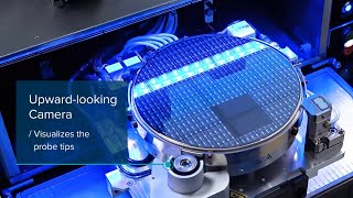
Media Summary: FormFactor's ReAlign™ technology for the SUMMIT200 ... Material the probes are made from 41:35 How to know where to probe the silicon 51:46 Why / how - The ability to grow high quality compound semiconductor material on Silicon has allowed exploitations of mature logic and ...
Wafer Probing - Detailed Analysis & Overview
FormFactor's ReAlign™ technology for the SUMMIT200 ... Material the probes are made from 41:35 How to know where to probe the silicon 51:46 Why / how - The ability to grow high quality compound semiconductor material on Silicon has allowed exploitations of mature logic and ... This video shows how these tests are carried out using Polytec's MSA Micro System Analyzer interfaced to a Since October 2020, ficonTEC has been hosting a series of 'products' and 'technologies/capabilities' webinars. The series ... Subscribe it to get more information! Camera Module System Semiconductor System www.techinspirit.co.kr.
Whether that's at +150 degrees C (or higher) or at sub-freezing temperatures, What is the process by which silicon is transformed into a semiconductor chip? As the second most prevalent material on earth, ... Kindly send us your detailed requirements Email: sales01.com , WhatsApp: Nicole +86 15889675465. At Complete Probe Solutions Inc., we take pride in being recognized by our customers as Dive into the intricate world of foundries with Advantest experts Keith Schaub and Shinji Hioki, as Shinji shares his extensive ... Watch How are BILLIONS of MICROCHIPS made from SAND? How are SILICON
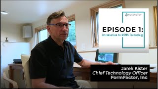
FormFactor's Chief Technology Officer Jarek Kister describes MEMS technology and how FormFactor uses sophisticated MEMS ...