Sponsored
Sponsored
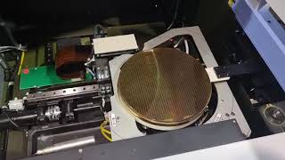
Media Summary: What does Technoprobe do? Probe cards, is the easy answer. But what is a probe card? Ok, this is a less easy question, but we'll ... Automated wafer probing with vertical probe cards on the summit200 probe station - FORMFACTOR ... Material the probes are made from 41:35 How to know where to probe the silicon 51:46 Why / how -

Wafer Testing - Detailed Analysis & Overview

What does Technoprobe do? Probe cards, is the easy answer. But what is a probe card? Ok, this is a less easy question, but we'll ... Automated wafer probing with vertical probe cards on the summit200 probe station - FORMFACTOR ... Material the probes are made from 41:35 How to know where to probe the silicon 51:46 Why / how - The ability to grow high quality compound semiconductor material on Silicon has allowed exploitations of mature logic and ... The CM300xi probe station is the perfect choice for accurate semi- and fully-automatic Dive into the intricate world of foundries with Advantest experts Keith Schaub and Shinji Hioki, as Shinji shares his extensive ...

Subscribe it to get more information! Camera Module System Semiconductor System www.techinspirit.co.kr. What is the process by which silicon is transformed into a semiconductor chip? As the second most prevalent material on earth, ... This webinar answers pre-submitted audience questions surrounding ATE ... for reliable contacting of Wafers in the Semiconductor industry. Plus, we offer custom solutions for all Step into the world of semiconductor manufacturing in this behind-the-scenes look at one of our 300mm

Photo Gallery

Semiconductor testing
What is a probe card (in 120 seconds) - Technoprobe
Automated wafer probing with vertical probe cards on the summit200 probe station - FORMFACTOR
How to probe the silicon inside of a chip | Explained by John McMaster
Silicon Photonics Wafer Level Test Measurement (Chinese) | FormFactor
Mechanical and Temperature Probing Challenges - FormFactor
Load Pull with CM300xi Automated Wafer Probe Station | FormFactor
Wafer-Level and Single-Die Testing
Wafer Testing Secrets You Did Not Know Yet
(Wafer Series) WAFER PROBE SYSTEM
MIMOS Failure Analysis - Wafer Level Testing
Wafer-level MEMS Optical Testing
View Detailed Profile
Semiconductor testing

Semiconductor testing

From

What is a probe card (in 120 seconds) - Technoprobe

What is a probe card (in 120 seconds) - Technoprobe

What does Technoprobe do? Probe cards, is the easy answer. But what is a probe card? Ok, this is a less easy question, but we'll ...

Sponsored
Automated wafer probing with vertical probe cards on the summit200 probe station - FORMFACTOR

Automated wafer probing with vertical probe cards on the summit200 probe station - FORMFACTOR

Automated wafer probing with vertical probe cards on the summit200 probe station - FORMFACTOR

How to probe the silicon inside of a chip | Explained by John McMaster

How to probe the silicon inside of a chip | Explained by John McMaster

... Material the probes are made from 41:35 How to know where to probe the silicon 51:46 Why / how -

Silicon Photonics Wafer Level Test Measurement (Chinese) | FormFactor

Silicon Photonics Wafer Level Test Measurement (Chinese) | FormFactor

The ability to grow high quality compound semiconductor material on Silicon has allowed exploitations of mature logic and ...

Sponsored
Mechanical and Temperature Probing Challenges - FormFactor

Mechanical and Temperature Probing Challenges - FormFactor

MEMS probe technology makes

Load Pull with CM300xi Automated Wafer Probe Station | FormFactor

Load Pull with CM300xi Automated Wafer Probe Station | FormFactor

The CM300xi probe station is the perfect choice for accurate semi- and fully-automatic

Wafer-Level and Single-Die Testing

Wafer-Level and Single-Die Testing

This video shows how these

Wafer Testing Secrets You Did Not Know Yet

Wafer Testing Secrets You Did Not Know Yet

Dive into the intricate world of foundries with Advantest experts Keith Schaub and Shinji Hioki, as Shinji shares his extensive ...

(Wafer Series) WAFER PROBE SYSTEM

(Wafer Series) WAFER PROBE SYSTEM

Subscribe it to get more information! Camera Module System Semiconductor System www.techinspirit.co.kr.

MIMOS Failure Analysis - Wafer Level Testing

MIMOS Failure Analysis - Wafer Level Testing

Wafer testing

Wafer-level MEMS Optical Testing

Wafer-level MEMS Optical Testing

Preciseley Microtechnology Corp.

‘Semiconductor Manufacturing Process’ Explained | 'All About Semiconductor' by Samsung Semiconductor

‘Semiconductor Manufacturing Process’ Explained | 'All About Semiconductor' by Samsung Semiconductor

What is the process by which silicon is transformed into a semiconductor chip? As the second most prevalent material on earth, ...

TSK UF3000 PROBER WAFER DUMMY TEST

TSK UF3000 PROBER WAFER DUMMY TEST

Used TSK UF3000 PROBER for sale -

Ask the Expert: ATE Testing

Ask the Expert: ATE Testing

This webinar answers pre-submitted audience questions surrounding ATE

FEINMETALL - Semiconductor Testing

FEINMETALL - Semiconductor Testing

... for reliable contacting of Wafers in the Semiconductor industry. Plus, we offer custom solutions for all

300mm wafer fab virtual tour

300mm wafer fab virtual tour

Step into the world of semiconductor manufacturing in this behind-the-scenes look at one of our 300mm

EEVblog #532 - Silicon Chip Wafer Fab Mailbag

EEVblog #532 - Silicon Chip Wafer Fab Mailbag

A look at some equipment and

TSK UF200 PROBER WAFER DUMMY TEST

TSK UF200 PROBER WAFER DUMMY TEST

Used TSK UF200 PROBER for sale -

How to Master Semiconductor Test Challenges

How to Master Semiconductor Test Challenges

Explore the evolution of semiconductor

Related Video Content

Wafer (electronics) - Wikipedia information

The wafer serves as the substrate for microelectronic devices built in and upon the wafer. It undergoes many...

WAFER Definition & Meaning - Merriam-Webster information

4 days ago · : a thin disk or ring resembling a wafer and variously used (as for a valve or diaphragm)

Sponsored