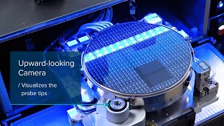
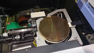
Media Summary: FormFactor's ReAlign™ technology for the SUMMIT200 Subscribe it to get more information! Camera Module System Semiconductor System www.techinspirit.co.kr. Step into the world of semiconductor manufacturing in this behind-the-scenes look at one of our 300mm
Wafer Probe - Detailed Analysis & Overview
FormFactor's ReAlign™ technology for the SUMMIT200 Subscribe it to get more information! Camera Module System Semiconductor System www.techinspirit.co.kr. Step into the world of semiconductor manufacturing in this behind-the-scenes look at one of our 300mm This video shows how these tests are carried out using Polytec's MSA Micro System Analyzer interfaced to a Watch How are BILLIONS of MICROCHIPS made from SAND? How are SILICON What is the process by which silicon is transformed into a semiconductor chip? As the second most prevalent material on earth, ...
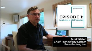
FormFactor's Chief Technology Officer Jarek Kister describes MEMS technology and how FormFactor uses sophisticated MEMS ...