Media Summary: As AI demands more "brain power" than ever before, the semiconductor industry is evolving, moving past the era of relying on ... 1. EMIB? : 2.5D vs. EMIB 2. Structure : Si bridge, metal layers, vias, RDLs, microbumps, C4 bumps 3. Process 4. Applications ... The next battle for chip design will be on interconnect and packaging, and to that end
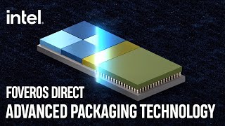
Eng Sub Intel Foveros - Detailed Analysis & Overview
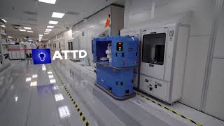
As AI demands more "brain power" than ever before, the semiconductor industry is evolving, moving past the era of relying on ... 1. EMIB? : 2.5D vs. EMIB 2. Structure : Si bridge, metal layers, vias, RDLs, microbumps, C4 bumps 3. Process 4. Applications ... The next battle for chip design will be on interconnect and packaging, and to that end The world's most intricate and high-tech package is one you'll likely never see. Once given little attention in chipmaking, packages ... Take a sneak peek “Behind This Door” to a critical level of # A “Behind this Door” video offers a peek into a small — but critical — piece of Intel’s manufacturing process: Assembly Test ...
PowerVia, an industry-first using a backside delivery scheme with optimized signal routing, reduction in power leakage and the ... PLEASE DON'T FORGET TO BE SUBSCRİBE FOR SUPPORT US.
![[Eng Sub] Intel Foveros](https://i.ytimg.com/vi/lT6Q1f6NhtI/mqdefault.jpg)


![[Eng Sub] Intel EMIB](https://i.ytimg.com/vi/hSQ_HAG2uoY/mqdefault.jpg)